NPN Transistor_ Just the same as the brain, computers contain billions of miniature cells called transistors. All are semiconductor devices made of silicon, a chemical compound found in the sand on a large scale. Since they were first invented, transistors have revolutionized many different industries as the electronic industries in on top. Transistor was invented by John Bardeen, William Shockley, and Walter Houser Brattain in 1947. They are many different types of transistors and can be categorized as PNP, NPN, JFET, and MOSFET.
Discover everything you need to know about NPN transistors on Linquip’s website. Linquip’s transistor experts are available to answer any questions you may have. Take the time to read Linquip’s “What Is a Transistor?” article.
Join Linquip as an Expert to take advantage of all Linquip has to offer. Would you be willing to write a Guest Post on Linquip? If yes, you can submit your content as a guest on the Linquip platform.
What is a Transistor?
Transistors are electronic components that are used in circuits for either amplifying or switching electrical signals or power and allowing them to be used in a large array of electronic devices. A transistor has two PN diodes combined back-to-back. Also, it has three terminals named emitter, base, and collector. The fundamental idea and physical law behind a transistor are that it should let you control the flow of current over one channel by varying the intensity of a much smaller current flowing through another channel.
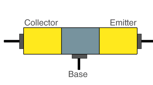
Terminals of Transistors
As discussed in the previous section, a transistor is composed of three terminals: emitter, collector, and base. In this section, we discuss the functionalities of each terminal in detail.
The base serves as a gate controller device for a larger electric supply. The collector is a larger electrical supply, and the outlet of that supply is the emitter. The current flowing through the gate from the collector can be regulated by sending varying levels of current from the base. In this manner, a very small amount of current can be used to control a large amount of current like in amplifiers. Transistor works as a switch or as an amplifier. As discussed before, a transistor is constituted of three terminals: emitter, base, and collector. In this part, we will discuss the operation of each terminal in detail.
The base works as a gate controller tool for a higher electric supply. The collector is a higher electrical supply, and the outlet of this supply is the emitter part. The current passing through the gate from the collector can be normalized by sending alternating levels of current from the base. As a result, a tiny amount of current can be used to control a considerable amount of current like in amplifiers. As mentioned before, transistors work as a switch or as an amplifier in the systems.
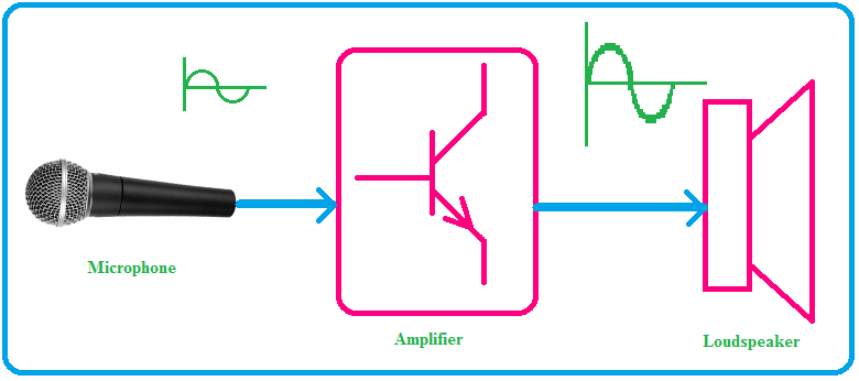
Physical Characteristics of Terminals can be described as below:
Emitter: this part of the transistor is on the left side of it. It is moderately sized and doped heavily.
Base: this segment is placed at the center of the transistor. It is thin and doped lightly.
Collector: this element is on the right side of the transistors. It is bigger than the emitter and is doped moderately.
Forward Biased Base-Emitter Junction
We have a flow of electrons (holes) in the direction of the emitter to base and holes (electrons) in the opposite direction from the base to emitter, but since the concentration of emitter electrons (holes) are more significant than the base holes (electrons), this current is mainly made of electrons (holes).
These emitter electrons (holes) grow minority carriers in the base; though, as the base is narrow, much little electron-hole recombination happens in the base, and these electrons (holes) are moved towards the collector-base junction.
Reverse Biased Collector-Base Junction
As these emitter electrons (holes) touch the collector-base junction, they are pulled across the junction into the electric field’s collector due to the ions’ depletion.
Varieties of Transistors and their Applications
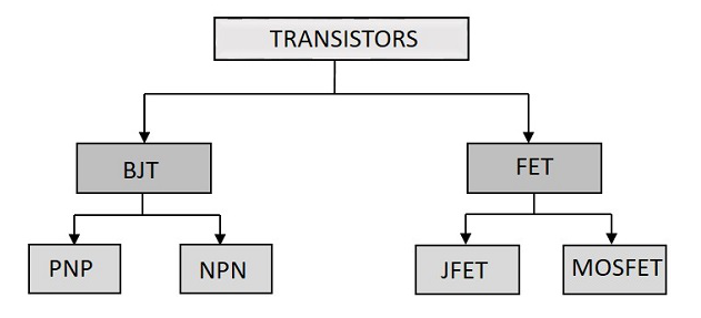
We have many types of transistors, and each transistor has its own special design due to its application. One of the main classifications of transistors is illustrated in the figure below:
Bipolar Junction Transistor
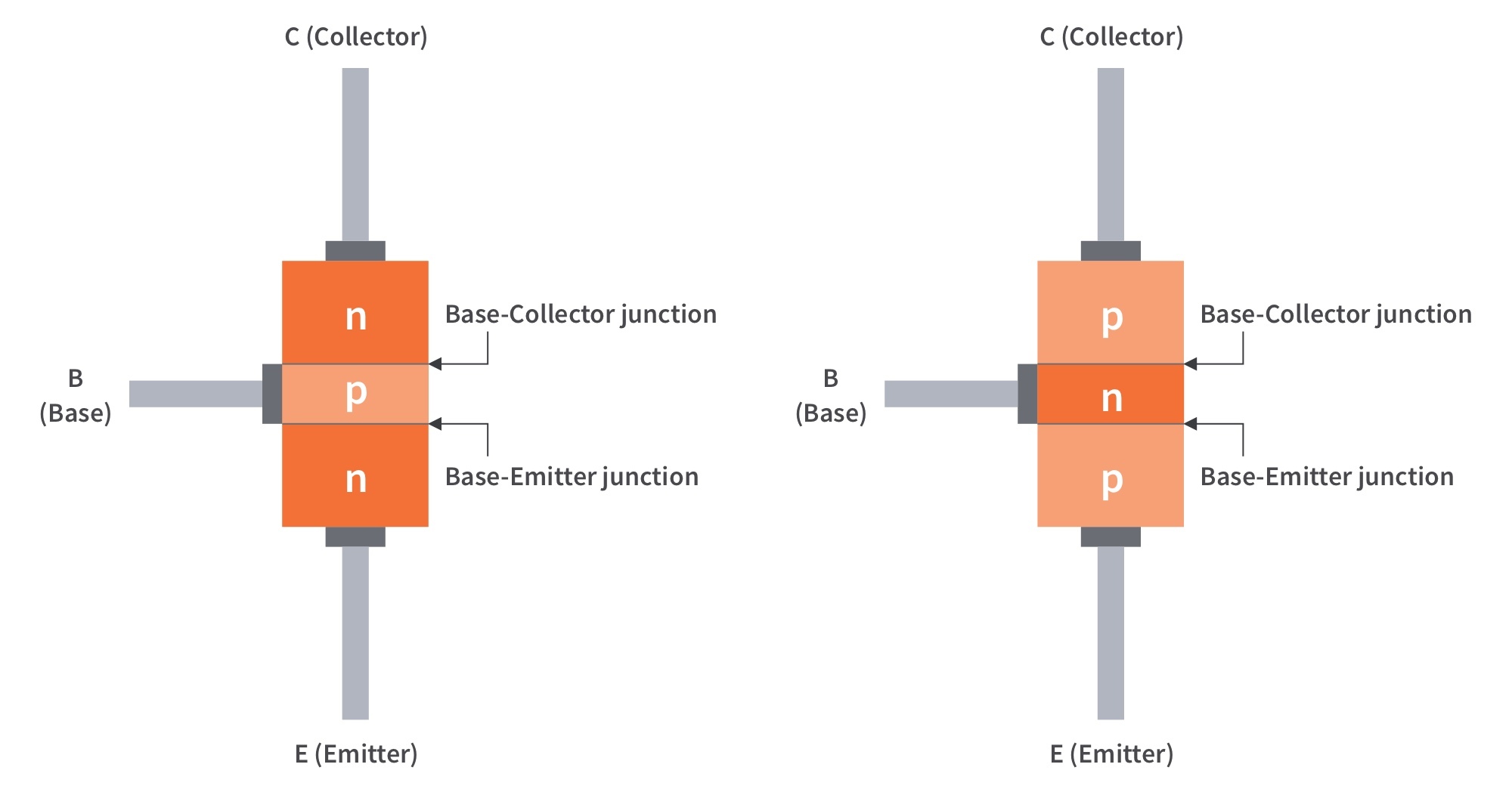
Bipolar junction transistors are shortly named BJT, are a current controlled device consisting of two PN junctions for its function. They are configured in two systems as PNP and NPN transistors. Among these two, the NPN transistor is the most chosen for the sake of convenience. The NPN transistor is built by placing a P-doped material between two N-doped materials. On the other hand, the PNP transistor is composed of placing an N-doped material between two P-doped materials.
Field Effect Transistor
Field-effect transistors are shortly called FET, are voltage-controlled devices, opposite to the BJT, which are current-controlled devices. The FET transistor is a unipolar device, and it means that all are made by using both p-type or n-type materials as the main substrate. One of the many advantages of them is that they all have a very high input impedance. The impedance of these types is in the order of Mega Ohms. Also, they have many other advantages, same as low power consumption and low heat dissipation.
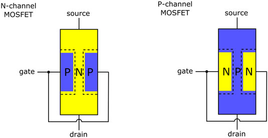
What are the Differences Between Bipolar Junction Transistor and Field Effect Transistor?
In this part, we will compare various differences between BJT and FET.
- The Bipolar Junction Transistor is a bipolar device, while the Field Effect Transistor is a unipolar device.
- The Bipolar Junction Transistor is a current-driven device, while the Field Effect Transistor is a voltage-driven device.
- The Bipolar Junction Transistors have low input impedance, while the Field Effect Transistors have High input impedance.
- The Bipolar Junction Transistors have Low noise level, while the Field Effect Transistors have a high noise level.
- The Bipolar Junction Transistors have Less thermal stability, while the Field Effect Transistors have good thermal stability.
While the transistor works as an amplifier, it serves as an energy booster. It comes in practical devices like hearing aids, as it is one of the prior gadgets we use for a transistor. Hearing aids include a tiny microphone that picks up sounds for your purpose and transforms them into varying electric currents. Also, Microphones are fed into a transistor that supports a miniature loudspeaker, and we hear a much louder version of noise around us.
Transistors also can work as a switch. An electric current flowing through one part of the transistors is able to make a much larger current flow in the other part, and this is the way all computer chips work. For example, a memory chip has hundreds of transistors, which each of them can be switched on or off separately. As every transistor can be in two different states, they can store two numbers of zero and one individually. A chip can use billions of transistors to keep billions of zeros and ones and as many letters and numbers as we need.
Applications of Transistor
Semi-conducting substances make the working of the transistors possible. Most of us may be familiar with electrically non-conductive and conductive materials. Metals are commonly considered to be conductive, while things same as plastics, wood, ceramics, and glasses are insulators or non-conductive. A team of engineers and scientists discovered how to use certain types of crystals and test them as electronic control devices by employing their semi-conductive properties.
Heat-Operated Switch
A thermistor is one of the essential components in the circuits of a heat-operated switch. It is a sort of resistor that responds to the around temperature. When the temperature gets higher value, its resistance decreases and vice versa.
A higher share of the supply voltage is decreased across R when the heat is applied to the thermistor, and the thermistor resistance drops. The base current rises and consequently followed by an increase in the collector’s current. As a result, the siren sounds, and the bulb glows. These special circuits are totally used in fire alarm systems.
Integrated Circuits
Integrated circuits have resistors, diodes, transistors, and capacitors combined with a thin wafer silicon chip, known as the microchips. Integrated circuits utilize less electrical power and occupy a small space that makes a small size circuit so that it can be built at a low cost.
What is NPN Transistor?
NPN transistor is one type of Bipolar Junction Transistor (BJT). The NPN transistor has two n-type semiconductor materials, and a thin layer of p-type semiconductor separates them. In this type of transistor, the majority of charge carriers are electrons. The flowing of electrons in the direction of the emitter to the collector forms the current flow in the NPN transistor. Generally, the NPN transistor is the most popular type of bipolar transistors and used much more because electrons’ mobility is higher than the mobility of holes. As discussed before, The NPN transistor has three terminals – emitter, base, and collector same as the other types. The NPN transistor is mainly used for amplifying and switching signals.
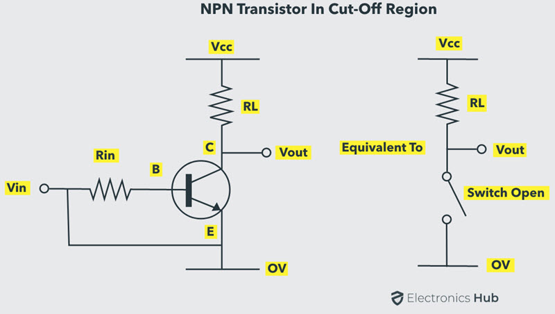
NPN Transistor Circuit
The figure below shows the symbol and structure of the NPN transistor. We can observe circuit currents, the three terminals of the transistor, and voltage value representations in this structure. Now we will discuss the operation of the NPN transistors.
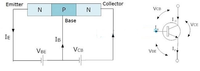
NPN Transistor Working
The figure below shows the NPN transistor circuit with resistive loads and supply voltages. The collector terminal always has a connection with the positive voltage. The emitter terminal has a connection with the negative supply, and the base terminal manages the ON/OFF states of the transistor based on the voltage applied to it.
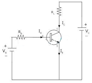
The working of the NPN transistor is very complex. As can be seen in the above circuit connections, the supply voltage VB is connected to the base terminal through the load RB. The collector terminal is connected to the voltage VCC through the load RL. Both RB and RL loads can limit the current flow by the corresponding terminals. In this system, the collector terminals and base terminals always have positive voltages with respect to the emitter terminal.
If the base voltage is equivalent to the emitter voltage, then the transistor is OFF. While the base voltage rises over emitter voltage, the transistor becomes more switched to be fully ON-state. If enough positive voltage is given to the base terminal, i.e. entirely ON state, the flow of electrons generated, and the current IC passes through the emitter to the collector. Now the base terminal works as input, and the collector-emitter region serves as the output.
It is necessary to have the positive collector voltage and greater than the transistor’s emitter voltage to have a proper current flow between the emitter and collector. There is some amount of voltage drop between the emitter and base, about 0.7V. As a result, the base voltage requirement is greater than the voltage drop of 0.7V; otherwise, the transistor will not work. The equation of the base current in a bipolar NPN transistor is:
I_{B} = (V_{B}-V_{BE})/R_{B}
where,
VB = Base bias voltage
IB = Base current
RB = Base resistance
VBE = 0.7V = Input Base-emitter voltage
The output collector current in the usual emitter NPN transistor is calculated by using Kirchhoff’s Voltage Law (KVL). The equation for collector supply voltage is presented as:
V_{CC}=I_{C}R_{L}+V_{CE}
From the above equation, the collector current for common emitter NPN transistor is given as
I_{C} = (V_{CC}- V_{CE})/R_{L}
In a usual NPN transistor, the relation between emitter current and collector current is presented as:
I_{C}=\beta I_{B}
In the active region, the NPN transistor works as a great amplifier. In a common emitter, the NPN transistor total current flows in the transistor are determined as the ratio of collector’s current to the base’s current as I_{C}/I_{B} . This ratio is also known as “DC gain” and doesn’t have units. This ratio is commonly expressed with β, and the maximum amount of β is about 200. In the base NPN transistor, the total current gain is defined with the ratio of collector current to emitter current as I_{C}/I_{E} . This ratio is known as α, and the value generally equals unity.
α, β and γ Relationships in NPN Transistors
There is a relationship between the two ratio parameters β and α, as will be discussed below.
α = Output current/Input current = DC current gain for base circuit
In a common base NPN transistor, collector current (IC) is output current, and emitter current is input current (IE).
\alpha =I_{C}/I_{E}
The value of the current gain (α) is very close to unity and a bit less than the unity. As we know, the emitter current is equal to the amount of small base current in addition to the large collector current:
I_{E}= I_{C} + I_{B}
I_{B}= I_{E} – I_{C}
Based on the previous α equation, the collector:
I_{c} = \alpha I_{E}
I_{B} = I_{E}-\alpha I_{E}
I_{B}= I_{E} (1-\alpha)
β = Output current/Input current = DC current gain for emitter circuit
Here collector current is output current, and base current is input current.
\beta = I_{C}/I_{B}
\beta = I_{C}/I_{E} (1-\alpha)
\beta = \alpha/(1-\alpha)
Base on the above equations we can present the relationship between α and β as:
\alpha= \beta(1-\alpha )=\beta/(\beta +1)
\beta =\alpha (1+\beta ) =\alpha / (1-\alpha )
The value of the β may vary in the range of 20 to 1000 for low-power transistors that operate in high frequencies. But generally, the value of the β may have values in the range of 50-200.
In the collector NPN transistors, the current gain is known as the ratio of the emitter current IE to base current IB. This current gain is defined as γ.
\gamma = I_{E}/I_{B}
As we know the emitter current is:
I_{E} = I_{C} + I_{B}
\gamma = (I_{C} + I_{B} )/I_{B}
\gamma = (I_{C}/I_{B}) + 1
\gamma = \beta +1
Here is the relationships between α, β and γ as below:
\alpha = \beta / (\beta +1)
\beta = \alpha / (1-\alpha )
\gamma = \beta +1
An Example for NPN Transistor
Here we want to calculate the base current IB to switch a 4mA resistive load of an NPN transistor. The current gain (β) value is 100.
I_{B} = I_{C}/\beta = (4\times 10^{-3})/100 =40uA
In the other case, for calculating the base current of an NPN transistor for the bias voltage of 10V and the base resistance of 200kΩ.
I_{B} = (V_{B}-V_{BE})/R_{B}
For the values of VB = 10V, VBE = 0.7V, VB = 10V, RB = 200kΩ.
By substitute of these values in the equation we have:
I_{B} = (V_{B}-V_{BE})/R_{B}= (10-0.7)/200kΩ = 46.5uA.
Common Emitter Configuration of NPN Transistor
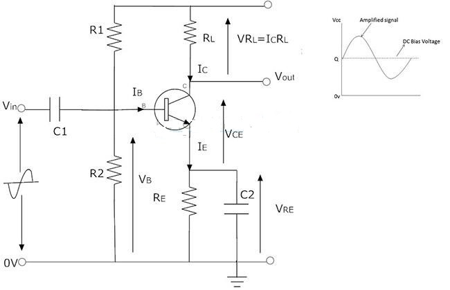
The typical emitter configuration circuits are one of the three BJT configurations. These standard emitter configuration circuits are employed as voltage amplifiers in systems. Generally, the BJT transistors include three terminals, but we need to take any of the terminals as common in the circuit connections. Consequently, we use one of these three terminals as the common terminal for both output and input actions. In this configuration, if we use the emitter terminal as a common terminal, it is called a common-emitter configuration.
This configuration is adopted as a single-stage common-emitter amplifier circuit. In this configuration base works as an input terminal, the collector is a terminal, and the emitter is a common terminal. The function of this circuit begins with biasing the base terminal, which forward biasing in the base-emitter junction. The little current controls the current flow in the transistor and in the base. This configuration always works in the linear region for amplifying the signals at the output side.
This common-emitter amplifier provides the inverted output and may have a very high gain. This gain value is affected by temperature and bias currents. The common-emitter amplifier circuits are the most used configuration compared to the other BJT configurations because of their low output impedance and high input impedance, and this configuration amplifier also provides high voltage gains and power gains.
The current gain of this configuration is always higher than unity, and the usual value is about 50. This configuration amplifier is mostly employed in applications where we need low-frequency amplifiers and radio frequency circuits. The diagram of the circuit for the common-emitter amplifier configurations is presented below:
Output Characteristics of NPN Transistor
The output characteristics curves of the bipolar transistor family are presented below. The curves show the relationship between the Collector-Emitter Voltage (VCE) and the collector current (IC) with respect to the varying base current (IB). The transistor is ‘ON’ when at least a small amount of current and a small amount of voltage is put at its base terminal relative to the emitter; if it is not, the transistor is in an ‘OFF’ state.
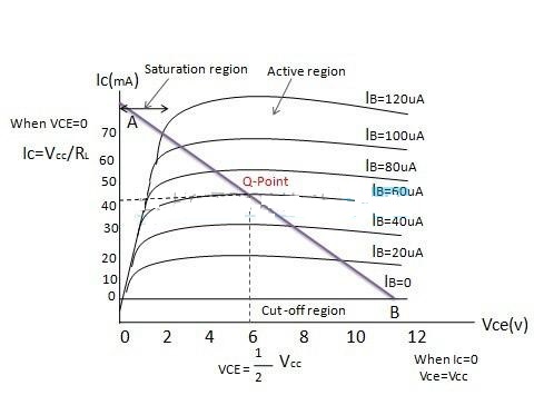
The collector current (IC) is mostly influenced by the collector voltage (VCE) at 1.0V level, but this IC value is not highly influenced above this value. As we know that the emitter current is the base currents addition to the collector currents: I_{E} =I_{C}+ I_{B} .
The current passing through the resistive load (RL) is the same as the transistor’s collector current. The equation for the collector current is presented as:
I_{C}= (V_{CC}-V_{CE})/ R_{L}
The straight line shows the ‘Dynamic load line’, which is joining points A (with VCE = 0) and B (with IC = 0). The region along this load line describes the ‘active region’ of the transistors.
The curves of the common-emitter configuration characteristics are employed to calculate the collector current in terms of the given collector voltage and base current. The red load line is used to define the Q-point in the graph. The slope of the red load line is proportional to the reciprocal load resistance: -1/RL.
NPN Transistor Applications
Here some applications of the NPN Transistors are listed:
- NPN transistors are primarily used in switching applications.
- NPN transistors are used in amplifying circuit applications.
- NPN transistors are used in the Darlington pair circuits for amplifying weak signals.
- NPN transistors are used in applications we need sinking current.
- NPN transistors are used in some classic amplifier circuits, the same as ‘push-pull’ amplifier circuits.
- NPN transistors are used in temperature sensors.
- NPN transistors are used in very High-frequency applications.
- NPN transistors are used in logarithmic converters.
FAQs about NPN Transistor
What can a NPN transistor be used for?
Circuits for amplification employ this part. It is utilized in Darlington pair circuits to enhance weak signals. Applications requiring a current sink employ NPN transistors. This element is used in some traditional amplifier circuits, such as “push-pull” amplifier circuits.
What is everything about NPN transistor?
Emitter, base, and collector are the three terminals of an NPN transistor. This transistor has two diodes that are wired in series. Emitter-base diode refers to the diode seen between the emitter-base terminal. Collector-base diodes are the type of diode that connects the collector and base terminals.
Why NPN type is the most widely used transistor?
Since electrons make up the majority of the charge carriers in NPN transistors, these devices have high electron mobility rates. For this reason, NPN transistors have superior conductivity to PNP transistors. NPN transistors are more favored for switching applications due to their quick switching rates.
Can we use NPN transistor as a switch?
Transistors of both types—NPN and PNP—can be used as switches. By biasing both NPN and PNP bipolar transistors using an “ON/OFF” static switch, it is possible to operate a basic terminal transistor differently from a signal amplifier. Solid-state switches are one of the principal applications for transistors that turn a DC signal “on” or “off.”
How does current flow in NPN transistor?
The base of an NPN transistor regulates how much current flows through it while still enabling current to flow from the emitter to the collector. On the other hand, PNP transistors are designed to allow current to go from the collector to the emitter.
Why is NPN used as an amplifier?
A forward bias must be given to a NPN transistor in order to utilize it as an amplifier. Therefore, holes migrate from the base to the emitter when a NPN transistor is utilized as an amplifier. Therefore, option D—holes travel from base to emitter—is the proper response.
Download What is NPN Transistor PDF
This article is available in PDF format for your convenience. To download, click the link below.
linquip.com-What is NPN Transistor Comprehensive Overview
Watch Videos about NPN Transistor
For more information about NPN Transistor, watch the following video.
Buy Equipment or Ask for a Service
By using Linquip RFQ Service, you can expect to receive quotations from various suppliers across multiple industries and regions.
Click Here to Request a Quotation From Suppliers and Service Providers
Read More In Linquip
- Types of Insulator Materials: 2021 Ultimate Guide
- What is a Fuse Wire & How Does It Work?
- What Is CNC Machining & How Does It Work? (A Comprehensive Guide)
- What is Electrical Identification? (Ultimate Guide)
- What is the Core Difference between Thermistor and RTD?
- What is a Paper Capacitor?
- What is Differential Pressure Sensor?: An Ultimate Guide
- What is Synchroscope? Method & Working Principles
- What is Ceramic Capacitor Used for?



Awesome explaination. I wished you could have been my college lecturer at the time. Thanks ever so much for your time and effort.
Thanks for visiting our website and leaving your comment, Tom! You are encouraged to visit Linquip Tech News, where you can find similar posts.
Such most impactful knowledge about transistors and it’s applications……..thank uh so much ..
Thanks for sharing your experience with us! You can also visit our industrial directories, where you can find thousands of various industrial equipment based on your application and demand.