One of the significant differences between forward and reverse biasing is that in forward bias, the battery’s positive terminal is connected to the p-type semiconductor materials, and the negative terminal has a connection with the n-type semiconductor materials. Whereas in reverse bias, the n-type material has a joint with the positive terminal of the voltage supply, and the p-type material is united to the battery’s negative terminal.
Biasing indicates that the potential difference or electrical supply is connected to the semiconductor devices. The potential difference has two types we know as the forward-bias and the reverse-bias. The forward bias overcomes the diode’s potential barrier and finds the easy path for current flow. On the other hand, in reverse bias, the potential difference increases the barrier’s strength, which limits the charge carrier from flowing across the junction. The reverse bias gives the high resistive path to the current flow, so no current flows through the circuit.
Working Principles of a Diode
The way that a diode functions can be hard to understand as it has relatively advanced quantum mechanics. However, in the simplest form, we can understand the operation of a diode by looking at the flow of positive charges (known as “holes“) and the negative charges (as we know, the electrons). Technically, a semiconductor diode is introduced as a p-n junction. We need these p-n junctions, and they have key roles in the operation of photovoltaic cells as well. Having a proper working diode needs a process known as doping. Semiconductor materials can be doped with different materials to have an excess of displaced electrons (frequently referred to as negative or n-type regions). They can also be doped with elements that form an excess of holes that absorb these electrons (frequently referred to as positive or p-type regions). The diode’s negative and positive regions are also the component’s cathode and anode, respectively.
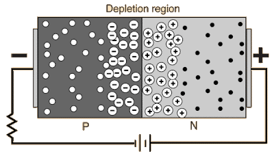
The different properties between these two materials and their interactions in a very short distance (less than a millimeter) make a diode when the two materials are joined. Combining these two kinds forms the p-n junction, and the zone between the two parties is called the depletion region. Electrons of the n-type region diffuse and Neutralized some of the holes in the p-type region. Now, we have negative ions in the p-type region and make positive ions in the n-type region as the figure represents. The response to electric fields depends on the direction of the electric field. All the discussed process leads to useful electronic action depending on which way the voltage or electric field is used, and all are called biasing.
What is Forward Voltage and Breakdown Voltage?
A minimum threshold voltage is needed to overcome the depletion region, which is a significant 0.7 volts for most silicon diodes. Furthermore, the reverse-bias voltage has a small amount of current through the diode named leakage current that is actually negligible in most purposes. Finally, a significant enough reverse voltage will result in the diode’s complete electronic breakdown and allow current to pass through the diode in the reverse direction.
In electronics, bias means a direction or the ability to flow in a particular direction, fundamentally when referring to a diode. Also, we describe biasing or bias within the electronics area as a methodology for establishing a set of voltages or currents at different points on an electronic circuit to establish proper operating conditions within an electronic element. Biasing also provides a circuit designer optimal control over a diode’s function.
What is Forward Biasing?
In forward biasing, the external voltage supply is applied across the PN-junction diode. This voltage cuts the potential barrier and provides a low resistance way to the flow of current. The meaning of the forward bias is the connection of the positive region to the p-terminal of the supply, while the negative region is joined to the n-type of the device.
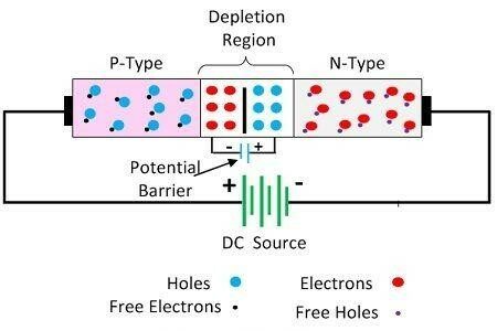
The potential barrier voltage has a tiny value (approximately 0.3 V for germanium and 0.7 V for silicon junction), so very little amount of voltage is needed for the complete elimination of the barrier potential. The entire elimination of the barrier creates a low resistance path for the current flow. Therefore, the current starts flowing into the junction. This current is named forward current.
What is Reverse Biasing
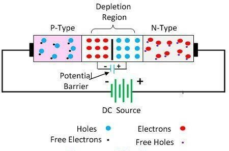
In reversed bias, there is a connection between the negative region and the positive terminal of the battery, and the positive region is joined to the negative terminal. The reverse potential boosts the strength of the potential barrier in this situation. The potential barrier resists the charge carrier flow across the junction. It builds a high resistive path that no current flows in the circuit.
What are the Differences Between Forward and Reverse Biasing?
Here is a list to help further highlight the distinctions between these two types:
- The forward bias decreases the strength of the potential barrier, and as a result, the current moves across the junction easily. whereas reverse bias increases the potential barrier and prevents the flow of charge carriers.
- In the forward biasing, we have a connection between the positive terminal and the battery to the p-region. Also, the negative terminal is connected to the n-type semiconductor materials. In the reverse bias, the positive terminal of the supply connects to the n-type materials, and the negative terminal is connected to the p-type semiconductor materials of the devices.
- The forward bias makes an electric field across the potential, which decreases the potential barrier’s strength, whereas the reverse bias enhances the potential barrier’s strength. (The potential barrier restricts the movement of electrons across the junction and is a layer between the PN-junction diode.)
- In the forward biasing, the anode’s voltage is higher than the cathode, whereas, in reverse bias, the cathode’s voltage is greater than the anode.
- The forward bias has a large forward current, while the reverse bias has a tiny forward current. (The current in the diode in the forward direction is named forward current.)
- The depletion layer of the diode is thick in reverse bias and very thin in forward biasing. (The depletion layer is the zone around the junction, free charge carriers are depleted.)
- The Forward bias reduces the diode’s resistance, whereas the reversed bias enhances the diode’s resistance.
- The current is easily flowing through the circuit in forward biasing, whereas reverse bias does not permit the current to flow through it.
- In the forward biasing, the current value is based on the forward voltage, whereas in reverse bias, the magnitude of the current is small or negligible.
- In the forward biasing, the device works as a conductor, whereas in the reverse bias, the device operates as an insulator.
Diagram for Forward and Reverse Biasing
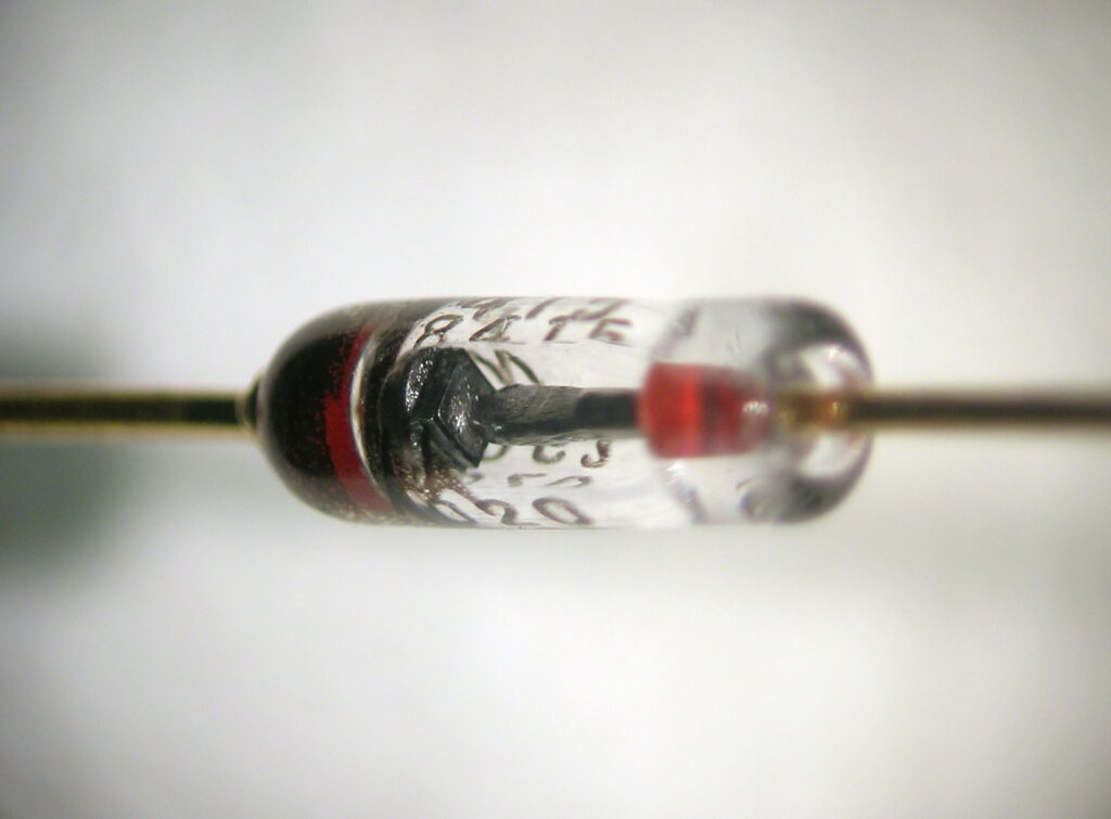
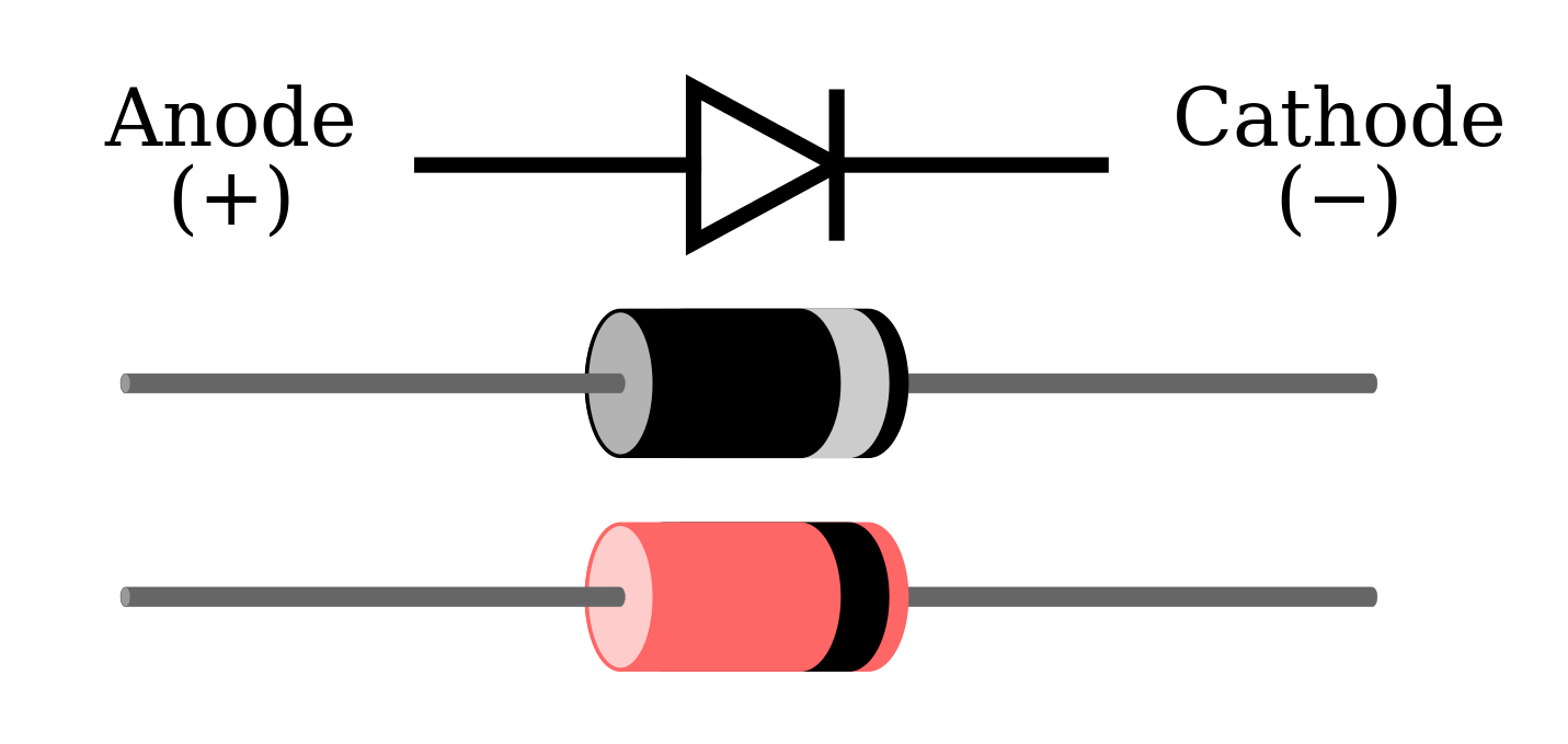
As discussed before, a diode is a two-terminal semiconductor device. It is something the same as an electronic valve, which allows current to flow in only one direction. The symbol of the diode is presented in the figure below. The symbol is arrow-shaped that shows the direction of the current that may flow. The terminal with a positive sign is known as the anode, while the terminal with a negative sign is named the cathode. The picture shows the physical device. They look like a resistor, except that they have a single band on one end. In forward-biased diodes, the current flows from the end without bands to the end of the cylinder.
When the voltage V is positive and greater than a minimum threshold voltage Vt, then the diode is called to be forward biased. A forward-biased diode conducts current in the direction illustrated in the figure. In this case of not being a diode forward biased, it is called reverse biased. A reverse-biased diode also conducts a current in the opposite sense of what is shown in the figure. However, this reversed current is extremely small so that the forward-biased diode is regarded as conducting, while the reverse-biased diode is known as not conducting. As it is used with a resistor, the diode is totally characterized once all know the relationship between the current and voltage. The diode’s IV characteristic can be found by the following equation:
i=I_{0}(e^{qv/kT}-1)
where q is the charge of an electron, k is Boltzmann’s constant equal to 1.381\times 10^{-28} J/K, and T is the material’s temperature in Kelvin. Usually, the reference current (I0) is very small, on the order of 10-9 or 10-15 amperes. Plotting the presented function leads to the IV characteristic given in the graph of the figure. This graph is the V-I curve as it shows how the current varies as a function of voltage.
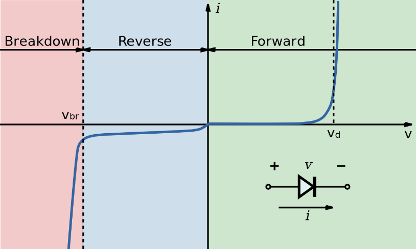
The diagram of the IV characteristic has three separate operating regions. The forward bias region is related to those positive voltages that are larger than a specified threshold level. The threshold voltage value, VT, depends on the physical properties of the semiconductor materials. Typical values for the threshold voltage are between 0.6 and 1.4 volts. For voltages that are lower than this threshold, the diode stops conducting. There is a little leakage of current that is in the orders of I0. But as mentioned earlier, the value of this current is minimal. If we decrease the voltage furthermore, we enter another region of working defined as the breakdown region.
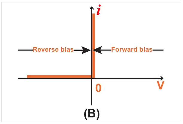
Usually, we use a diode in either its reverse or forward biased modes. In particular, we simplified this behavior, and then we can consider the diode as an open valve when the voltage is greater than the threshold voltage VT and is closed if it is less. These considerations lead to the simplified I-V characteristic diagram that is shown in the figure below with the threshold V of the zero. In this idealized plot, we can see the reverse bias region is simplified so that we have zero current passing in this region if v< V_{T} .
If we have a forward-biased diode, then the current is probably unbounded, which indicates that the diode works as a short circuit. In other words, a forward-biased diode operates the same as a short circuit, and a reverse-biased diode performs like an open circuit.
What is Light-Emitting Diode Bias Type?
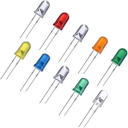
An LED is a light-emitting diode. The LED emits light in terms of being forward-biased, and it has no light whenever it is reverse-biased. The intensity of the emitted light is equal to the square of the current flowing in the device. The figure below displays a picture of an LED. Same as the other diodes, these LEDs have two heads, and one lead is longer than the other one. They are presented in this form to indicate which end of the diodes are anode (positive) and which ones are cathode (negative). The longer lead is positive in numerous types, but we can quickly test this by connecting the LED to a voltage supply same as a battery and knowing which adjustment causes the LED to emit light.
Summery
The forward and reverse biasing can be distinguished by the below parameters:
Definition of the Forward and the Reverse Biasing
The external voltage supply, which is applied across the PN-diode for defeating the potential barrier to constitutes the easy flow of current through it, is named forward bias.
The external voltage supply, which is applied to a PN-junction for increasing the potential barrier and limits the flow of current through it, is named reverse bias.
Symbols of the Forward and the Reverse Biasing and Their Connections
The battery’s positive terminal is connected to the P-type semiconductor part of the device, and the negative terminal is connected to the N-type semiconductor material in the forward bias.
In reverse bias, the battery’s negative terminal is connected to the P-region, and the positive terminal of the battery is connected to N-type semiconductor material.
Voltage Value in the Forward and the Reverse Biasing
The voltage of anodes is greater than cathodes in the forward biasing, and by increasing this voltage, barrier potential reduces. The voltage of the cathodes is greater than an anode and strengthens barrier potential.
Depletion Layer and Resistance in the Forward and the Reverse Biasing
We have thin depletion layers in the forward biasing, and it has low resistance. On the other hand, the depletion layer’s thickness is high in the reverse biasing and has high resistance.
The Magnitude of Current and Operation State in the Forward and the Reverse Biasing
The forward biasing allows the current to pass, and the magnitude of this current depends on the forward voltage, so it acts as a conductor. The reverse biasing prevents the current from passing, and the magnitude of this current is zero, so it works as an insulator.
Buy Equipment or Ask for a Service
By using Linquip RFQ Service, you can expect to receive quotations from various suppliers across multiple industries and regions.
Click Here to Request a Quotation From Suppliers and Service Providers
Read More In Linquip

