Both p-type and n-type semiconductor are the kind of extrinsic semiconductors. The primary factor that makes differences between p-type and n-type semiconductors is their doping material. The addition of group III elements forms a p-type semiconductor material, or we can say trivalent impurity to a pure (intrinsic) semiconductor. In contrast, the n-type semiconductor material is formed by adding group V elements, i.e. a pentavalent impurity, to a pure or intrinsic semiconductor.
Some other factors also exist that generate significant differences between p-type and n-type semiconductors, which we will address these differences between p-type and n-type semiconductors in detail. But, before talking about the differences between P-Type and N-type semiconductors, take a look at a more detailed definition of semiconductors and also p-type and n-type semiconductors.
Depending on your application, you can find all the information you need about P-type or T-type semiconductors on Linquip’s website. We have a team of experts at Linquip ready to answer any questions you may have about these types of devices. Check out Linquip’s article, “What Is Semiconductor?” to learn more about these pieces of equipment.
Additionally, you can register as a Linquip Expert and have access to all services Linquip has to offer. Would you like to publish a Guest Post to Linquip? The Linquip platform allows you to submit your content as a guest.
What Is a Semiconductor?
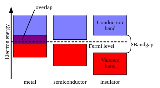
A material that has a conductivity among that of a conductor and an insulator is called a semiconductor. Energy levels are interpreted in terms of bands in the band theory of solids. Under this theory, for material to manage, electrons from the valence band should be able to drive up to the conduction band (note that “driving up” here does not indicate an electron physically moving up, but rather an electron getting an amount of energy that is connected with the energies of the conduction band).
According to the theory, metals, conductor materials have a band structure where the valence band overlays with the conduction band. As a consequence, metals can easily conduct electricity. In insulators, the bandgap between the valence band and the conduction band is pretty large so that it is tough for electrons to get into the conduction band.
In contrast, semiconductors have a tiny gap between the valence and conduction bands. By raising the temperature, it is possible to give electrons enough energy that enables them to travel from the valence band up to the conduction band. Later, the electrons can go in the conduction band, and the semiconductor can conduct electricity.
Intrinsic semiconductors are components with four valence electrons per atom, i.e. elements that happen in “Group-IV” of the periodic table, such as germanium (Ge) and silicon (Si). Each atom has four valence electrons. Each of these valence electrons can create a covalent bond with one of the valence electrons in a neighboring atom.
All of the valence electrons are included in a covalent bond. Rigorously speaking, this is not the case: depending on the temperature, several electrons can “break” their covalent bonds and take part in conduction. However, it is possible to significantly increase a semiconductor’s conducting ability by adding small quantities of an impurity to the semiconductor, in a manner designated doping. The impurity, which is added to the intrinsic semiconductor is named the dopant. A doped semiconductor is committed to as an extrinsic semiconductor.
P-Type Semiconductor
P-type semiconductors are produced by doping an intrinsic semiconductor with an electron acceptor element throughout manufacture. The term p-type regards the positive charge of a hole. As opposed to n-type semiconductors, p-type semiconductors have a bigger hole concentration than electron concentration.
In p-type semiconductors, cavities are the majority carriers and electrons are the minority carriers. A typical p-type dopant for silicon is aluminum, boron, or gallium. For p-type semiconductors, the Fermi level is underneath the intrinsic Fermi level and lies closer to the valence band than the conduction band.
Let us have a look at the below figure that describes doping of aluminum to a pure silicon material:
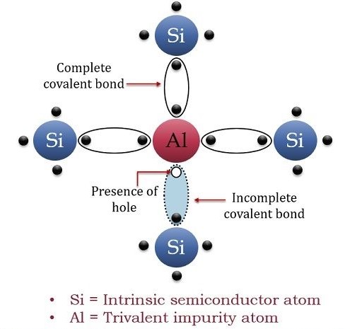
An aluminum atom contains three electrons at its valence shell. Moreover, silicon has a total of four electrons at its valence shell. So, three valence electrons of an aluminum atom form covalent bonds with three electrons of silicon. Nevertheless, in this case, a vacancy of an electron (or a hole) appears. The translation of this hole is mostly responsible for the conduction in the p-type semiconductor to take place. Therefore, in this case, charge carriers are holes rather than electrons.
Let’s have a look at the energy level diagram of a p-type semiconductor:
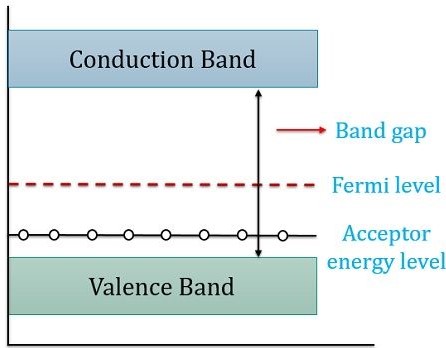
Here, we can recognize that the Fermi level is being near the valence band. It is evident from the above figure that there is a tiny energy difference between the valence band and the acceptor energy level. Hence, electrons easily drift to the acceptor energy level producing a vacancy of electrons. Therefore, making holes in the valence band.
N-Type Semiconductor
N-type extrinsic semiconductors are created when group V elements like phosphorus, antimony, bismuth, etc., are doped to a complete semiconductor crystal. These are named so because doping these elements will create an additional electron in the atom’s valence shell.
The figure below depicts the doping of phosphorus element into a pure silicon material:
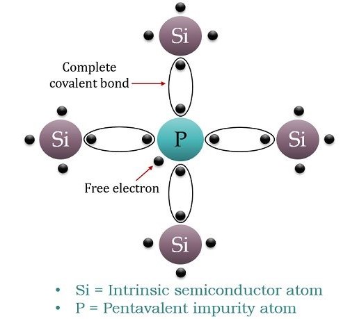
We previously comprehend that phosphorus consists of 5 electrons at its valence shell. When it is doped with pure silicon with 4 electrons at the valence shell, it forms four covalent bonds. This causes the presence of an unbounded electron that is kept free to move into the conduction band. This electron is perceived as a free electron and its progress raises the conductivity of the material.
Let’s take a look at the energy band diagram of N-type semiconductor:
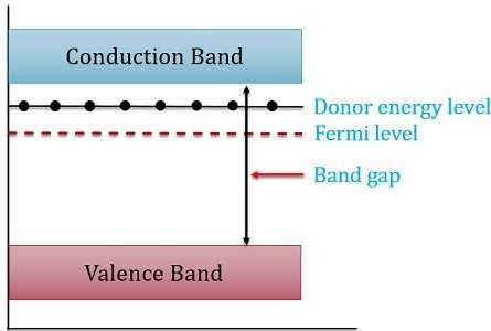
Here, from the figure, it is clear that the presence of the Fermi level is near the conduction band. We can recognize that a small energy difference exists between the donor energy level and the conduction band. So, less energy is required by the electrons to reach the conduction band.
Key Differences between P-Type and N-Type Semiconductor
In what follows, we itemized the key differences between p-type and n-type semiconductors:
- A p-type semiconductor is created when group III elements are doped to a complete semiconductor material. As opposite, an n-type semiconductor is created when group V elements are doped to an intrinsic semiconductor.
- As components like gallium, boron, indium, etc., are doped to form a p-type semiconductor; therefore, it creates an additional hole, thus also known as acceptor atom. On the contrary, components like bismuth, arsenic, antimony, etc., are doped to have an n-type semiconductor, creating an additional electron, thus also termed as donor atom.
- Another factor that makes critical differences between p-type and n-type semiconductors is that in p-type semiconductors, holes are the majority carriers. While in the case of an n-type semiconductor, electrons behave as majority carriers.
- The minority carriers in the case of the p-type semiconductor are electrons, whereas, in that of n-type semiconductors, these are holes.
- The conductivity of the device depends mainly on the majority of carriers. Hence in the p-type semiconductor, holes are subject to current conduction. On the contrary, in the case of an n-type semiconductor, electrons are responsible for current conduction.
- In the case of a p-type semiconductor, the fermi-level appears closer to the valence band than that of the conduction band. On the contrary, the Fermi level in the case of an n-type semiconductor exists near the conduction band.
- The collection of holes is more than electrons in the case of p-type semiconductor material. This is while in n-type semiconductors, the concentration of electrons is more significant than gaps.
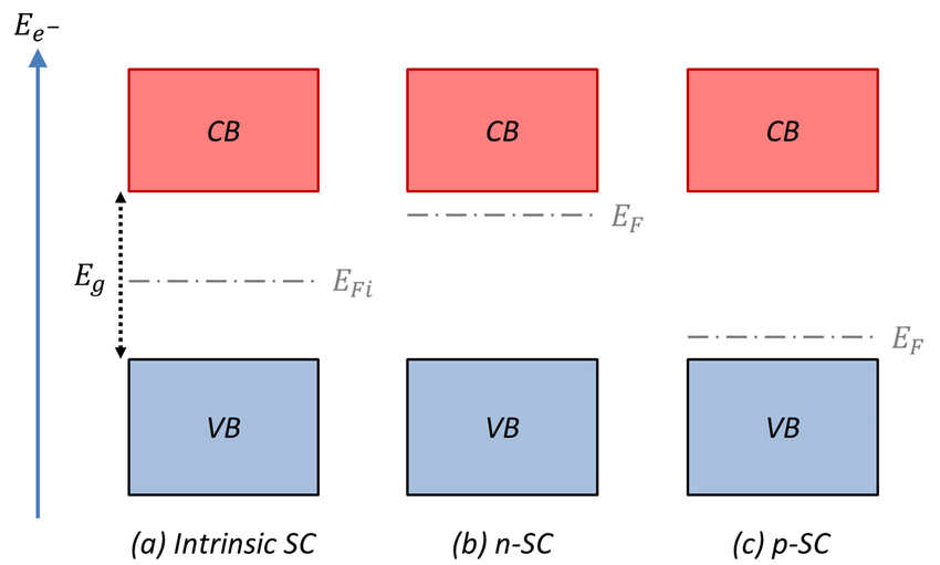
Here we mentioned some key differences between p-type and n-type semiconductors. In continuation, we propose a summarized comparison chart about differences between p-type and n-type semiconductors.
Comparison Chart
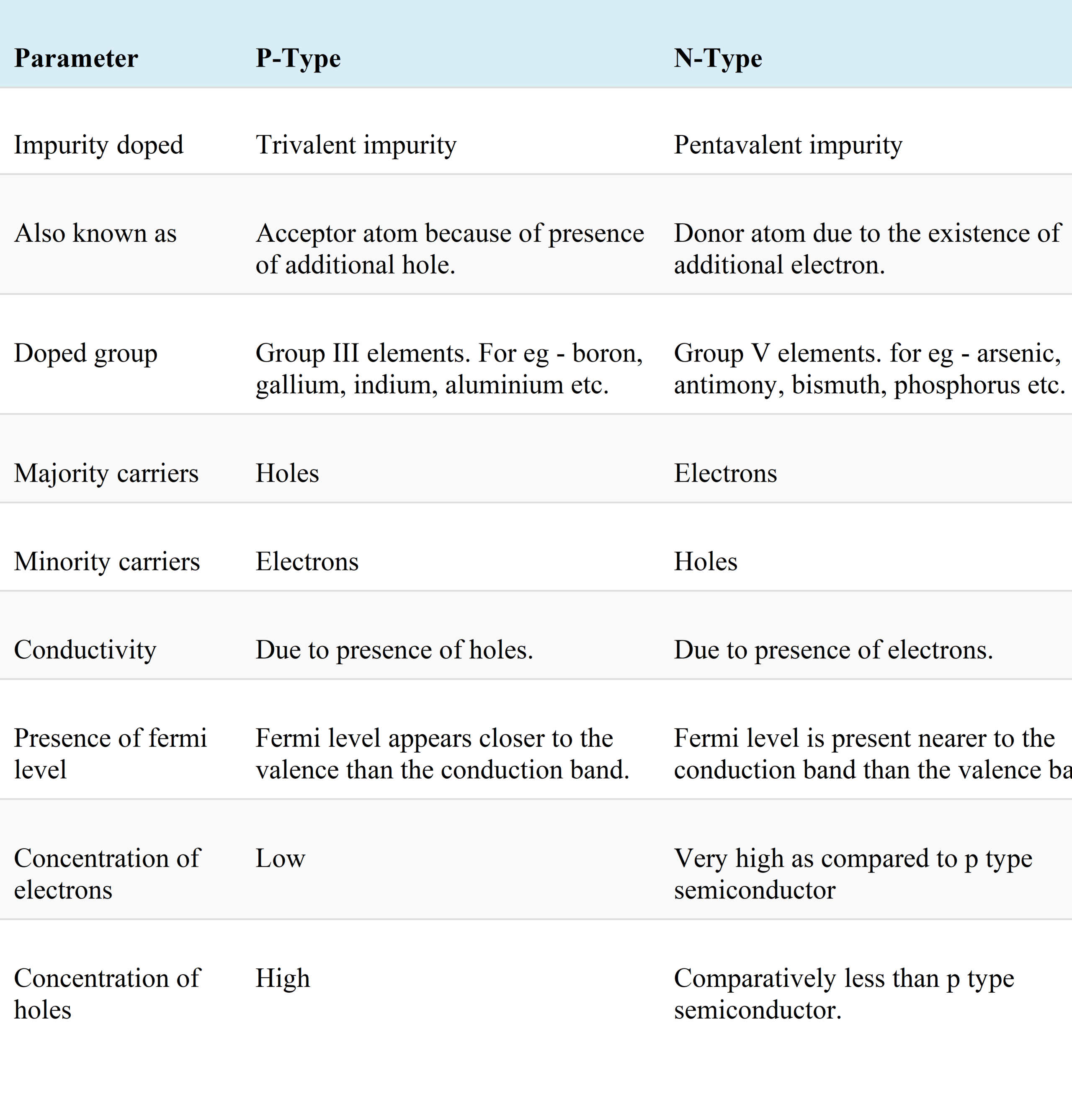
Here is a comprehensive chart that compares the main differences between p-type and n-Type semiconductors.
What Are the Examples of N-Type and O-Type Semiconductors?
An n-type semiconductor is created by introducing a pentavalent impurity for doping. An example of pentavalent impurity is phosphorus or arsenic. When trivalent impurities are used for doping, p-type semiconductors are formed. Aluminum and boron are examples of trivalent impurities.
What Are the Similarities between N-Type and P-Type Semiconductors?
N-type and P-type semiconductors are both intrinsic semiconductors. While they fall under the same category of extrinsic, their behaviors are very different based on their dopants. Nevertheless, Fermi levels are positioned towards conduction or valence bands, depending on the type.
Download P-Type vs N-Type Semiconductors PDF
You can download this article to your hard drive as a PDF document so that you can access this content whenever you need it.
Conclusion
So, from the above examination, we can conclude that a p-type semiconductor is abbreviated due to the fact that these are positive semiconductors because of extra holes. In contrast, n-type semiconductors are termed as negative semiconductors because of the presence of extra electrons.
Buy Equipment or Ask for a Service
By using Linquip RFQ Service, you can expect to receive quotations from various suppliers across multiple industries and regions.
Click Here to Request a Quotation From Suppliers and Service Providers
Read More In Linquip
- HVDC vs HVAC Transmission Systems– Difference between them
- Top USA and International Semiconductor Manufacturers in 2022
- What are the Differences Between Series and Parallel Circuits?
- What are the Differences Between Forward and Reverse Biasing?
- Solid vs Stranded Wire (A Practical Guide)
- What is a Fuse Wire & How Does It Work?
- Types of Electrical Wire + Application (Complete Guide)
- Top 10 Machine Shops in Tampa in 2022 (Clear Guide)
- 10 Types of Molding Machinery + PDF (Clear Guide)
- 3 Common Types of Electrical Connectors (Clear Guide)
- Types of Sensors Detectors/Transducers: An Entire Guide
- Top Bearing Suppliers in USA & Worldwide in 2022
- 15 Types of Electrical Power Connectors (Clear Guide) + PDF
- The 8 Best Circuit Breaker Locators in 2022



Your advice has been very useful when it concerns recognizing solar power – thanks for always being a source of knowledge and assistance! We’re below as a group, so allow’s proceed the great discussion we have actually started on. If there’s something concerning solar power that rate of interest you, do not think twice to connect– your input is more than welcome.
Thanks for visiting our website. You can visit our Industrial Equipment page, where you can find various pumps based on your application and demand. You can also visit our expert page and take advice from hundreds of professionals on your issue.